This project was completed for EEEE 120. Publishing the graded deliverables — including the state diagram and state table, Karnaugh maps, minimised equations, and gate-level schematics — would violate RIT's Academic Honesty Policy. This page therefore explains the design, implementation process, and verification results without reproducing the artefacts submitted for grading.
01Purpose and operation
A bit-serial adder–subtractor performs addition or subtraction on two five-bit operands, processing one bit position per clock cycle rather than all five positions simultaneously.
A conventional five-bit parallel adder requires five full adders. The serial design reuses a single full adder five times, storing the carry between clock cycles. This creates a direct trade-off between hardware and execution time: the circuit uses less arithmetic hardware, but requires five cycles to produce a result.
The reduction in arithmetic hardware comes with an added control requirement. The design needs registers that can load and shift, a carry-storage element, and a controller that determines when to load the operands, when to shift them, and when the operation is complete. Designing that controller was the central challenge of the project.
The circuit accepts two five-bit parallel inputs, a control signal selecting addition or subtraction, a start signal, a clock, and a reset. It produces a five-bit result and a Done signal.
02Serial arithmetic and carry propagation
Binary addition processes one column at a time, just as decimal addition does. A half adder combines two bits and produces a sum and a carry. A full adder combines two operand bits with a carry-in from the previous column, allowing multiple columns to be connected in sequence.
| Xi | Yi | Cin | Sum | Cout |
|---|---|---|---|---|
| 0 | 0 | 0 | 0 | 0 |
| 0 | 0 | 1 | 1 | 0 |
| 0 | 1 | 0 | 1 | 0 |
| 0 | 1 | 1 | 0 | 1 |
| 1 | 0 | 0 | 1 | 0 |
| 1 | 0 | 1 | 0 | 1 |
| 1 | 1 | 0 | 0 | 1 |
| 1 | 1 | 1 | 1 | 1 |
In a parallel ripple-carry adder, the carry propagates through multiple full adders in a single cycle, and the length of that combinational path limits the maximum clock frequency. In the serial design, the carry propagates through time instead: the carry-out from one cycle is stored in a flip-flop and used as the carry-in during the next.
As a result, the combinational path is only one full adder deep, regardless of operand width. A wider serial adder would require more cycles and larger registers, but not additional full adders.
Because binary addition begins with the least significant bit, both operands are stored in shift registers. During each active clock cycle, the current least significant bits of X and Y, along with the stored carry, enter the full adder. The resulting sum bit is shifted into the accumulator, and the carry flip-flop is updated. After five cycles, every bit has passed through the full adder once and the accumulator contains the result.
03Subtraction without a separate subtractor
The circuit performs subtraction using two's-complement arithmetic rather than a dedicated subtractor:
Each bit of Y passes through an XOR gate controlled by the Sub signal. When Sub is low, the XOR leaves the bit unchanged; when it is high, the XOR inverts it. This allows the same register to provide either Y or its complement, depending on the selected operation.
The required +1 is supplied through the initial carry-in. When subtraction is selected, Sub presets the carry flip-flop so that the first addition begins with a carry-in of one. This implements the two's-complement correction without requiring a second adder, an incrementer, or an additional clock cycle.
At the end of the operation, the done state clears the carry flip-flop while holding the result. This prevents a carry from one operation from affecting the next.
04System architecture
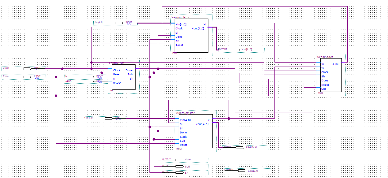
The design consists of four major blocks. Each block was developed and simulated independently before being integrated into the complete circuit.
X accumulator
The X accumulator is a shift register that initially stores the X operand and eventually stores the result. Each register stage uses a 4-to-1 multiplexer controlled by the controller's Done and Sh signals. These controls allow the register to load the parallel input, shift during an operation, or hold its current value. The hold operation routes each flip-flop's output back to its input, keeping the result stable after the operation completes.
Y shift register
The Y register uses a similar structure, but its parallel input passes through the XOR inversion bank controlled by Sub. Its output is fed back to the input so that the register rotates rather than discards bits as it shifts.
After five shift cycles, the register has returned to its original bit pattern. This also provides a useful check that all five bits circulated through the datapath exactly once.
Serial adder
The serial adder consists of one full adder and a carry flip-flop. The carry flip-flop stores the carry-out from one cycle and provides the carry-in for the next. It advances only while shifting is active.
Control FSM
The control block is a finite-state machine that generates the Sh, Sub and Done signals. It coordinates loading, subtraction setup, serial shifting, and result hold.
05The controller
The controller contains eight states: one idle-and-load state, one subtraction-setup state, five shift states, and one done state.
It is implemented as a Moore machine, so its outputs depend only on the current state rather than directly on the inputs. This matters because the control signals drive multiplexer selects and flip-flop presets throughout the datapath. With a Moore machine, those signals change only when the state changes, which makes the timing more predictable and reduces the possibility of input-dependent glitches.
The sequence is fixed and does not depend on the operand values. The controller begins in the idle state, where both operand registers load their parallel inputs. When the start signal is asserted, the machine advances to the setup state, where Sub is asserted only when subtraction has been selected. The controller then passes through the five shift states and finally enters the done state, where the registers hold their values, the carry flip-flop is cleared, and the result remains stable until the next operation begins.
Two design decisions
Gray-coded state assignment. The eight states were assigned Gray-coded values so that adjacent states differ by only one state bit. During a normal transition, only one state flip-flop changes, reducing the possibility of transient decoding behaviour. I chose Gray coding over binary or one-hot encoding because the state sequence is primarily linear.
Explicit handling of a don't-care condition. The value of Sub does not affect the datapath during the shift or done states; it is only needed during subtraction setup. Although those entries could have been left unspecified for logic minimisation, I set them explicitly to zero. This prevents the minimised logic from asserting Sub during states where it has no useful function, and makes the resulting waveforms easier to interpret during debugging.
The next-state and output logic were derived by hand using six Karnaugh maps: three for the next-state bits and three for the controller outputs. The minimised equations were then implemented as gates driving the three state flip-flops.
06Design process and tools
The circuit was entered as schematics in Quartus Prime and verified using Quartus's simulator and ModelSim. The design process followed a fixed sequence:
- Specify the required behaviour.
- Construct the state diagram.
- Build the state table.
- Select a state encoding.
- Minimise the next-state and output logic.
- Enter each block as a schematic.
- Simulate each block independently.
- Integrate the blocks.
- Verify the complete circuit.
One issue involved the clock polarity of the flip-flops. The design required negative-edge triggered behaviour, while Quartus's DFF primitive is positive-edge triggered. The circuit could still compile and simulate, but its behaviour was offset from the intended timing.
I corrected the problem by wrapping the primitive with an inverted clock, so the internal flip-flop received a rising edge precisely when the system clock fell. This was a small implementation detail, but it highlighted an important lesson: the default behaviour of a library component has to be checked rather than assumed to match the design specification.
07Verification
Verification was performed in three stages. Each block was tested independently before the complete circuit was assembled, ensuring that a top-level failure could be traced to a specific source.
- Functional simulation verified the logical behaviour with propagation delays ignored. Each block's waveforms were compared against the behaviour specified in the project requirements.
- Timing simulation repeated the same tests with delays annotated, confirming that signals settled before the following active clock edge.
- Exhaustive simulation tested the completed circuit in ModelSim against a reference comparator, for every combination of the two five-bit operands and the add/subtract control input.
The circuit was verified entirely in simulation and was not programmed onto a physical board. Consequently, the project does not include place-and-route results, FPGA resource utilisation, or measurements from hardware. The results described here are predictions from the simulation tools.
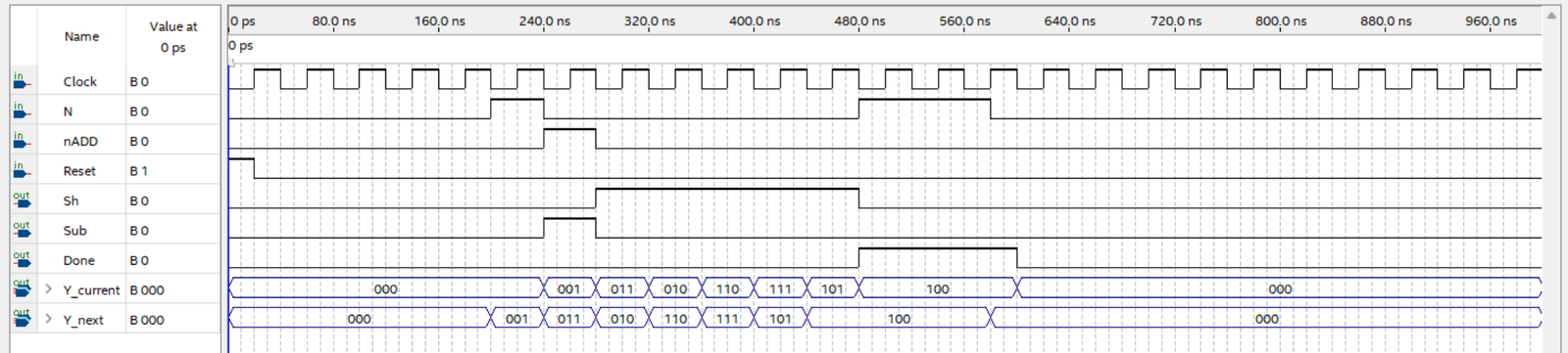
The exhaustive test used an EQUAL signal that asserted whenever the circuit's output matched the reference result. The verification condition was that EQUAL remained high whenever Done was asserted. This condition held for every combination of operands and operation type.


Worked example
Take X = 01011 (11) and Y = 00101 (5), with subtraction selected.
During the setup state, the XOR bank inverts Y and the carry flip-flop is preset. Together, these operations form the two's-complement representation of −Y. The five shift states then add one bit pair and the stored carry during each cycle.
When the controller reaches the done state, the accumulator contains 00110 — six, the expected result of 11 − 5. The Y register has also rotated back to the pattern it held immediately after setup, which provides an independent check that all five positions shifted correctly without losing any bits.
08Results and lessons
The completed circuit performed five-bit addition and subtraction correctly for every input combination tested. Subtraction was implemented through two's-complement arithmetic, allowing the design to reuse the same serial full adder for both operations. Functional and timing simulations of the individual blocks matched the specified behaviour before top-level integration.
The project reinforced the importance of following a structured sequential-design process: define the behaviour, create the state diagram and table, choose an encoding, minimise the logic, implement the circuit, and then verify it. Testing each block independently was especially valuable, because it made failures easier to isolate.
The two main implementation issues both came from assuming that default behaviour matched the design intent. The first involved the clock polarity of the flip-flop primitive. The second involved leaving a controller don't-care unspecified and allowing the logic minimiser to choose its value. Both problems were straightforward to correct once identified, but they were more difficult to locate because the circuit still compiled and produced plausible waveforms. The experience reinforced the value of making hardware behaviour explicit, even when a detail appears inconsequential.